Waveguides are structures that direct electromagnetic waves from one point to another efficiently. They excel at handling high-frequency signals while minimizing loss. This article delves into the principles, types, and diverse applications of waveguides.
Key Takeaways
- Waveguides are critical for directing and confining electromagnetic waves, significantly reducing signal loss and improving transmission efficiency, especially at high frequencies.
- There are three primary types of waveguides: rectangular, circular, and dielectric, each with unique properties suited to different applications and frequency ranges.
- Waveguide technology has broad applications, including microwave communications, optical fiber networks, and medical uses, highlighting its versatility and importance in modern technology.
Basics of Waveguides

Fundamentally, waveguides are engineered structures that serve to:
- Contain and steer electromagnetic waves down a designated course
- Excel in transmitting signals at high frequencies
- Keep signal degradation to a minimum
- Operate as conduits for electromagnetic energy, transferring it from its origin point to the intended target with notable proficiency.
Waveguide technology’s evolution is deeply connected with the rapid progress made in telecommunications throughout the early part of the 20th century. Pioneering work by scientists at MIT and Bell Labs led to their independent invention during the 1930s, recognizing an urgent requirement for better transmission methods of signals at higher frequencies. Their innovations set up what would become foundational technologies for modern systems used in microwave communications and millimeter-wave transmissions, leading to transformations across domains such as radar systems and satellite broadcasting.
Despite their different shapes, all waveguiders adhere to a key concept: they trap electromagnetic energy within a specific area. For microwaves specifically, these are typically hollow metallic tubes with rectangular or cylindrical cross-sections which bounce electromagnetic waves back-and-forth along conductive surfaces allowing them efficient passage from input point to exit point without substantial losses. The specifications regarding size and materials chosen for constructing waveguides are meticulously selected based on suitability for certain frequency bands—proving especially advantageous when dealing with frequencies over 1 GHz up through several hundred gigahertz range.
Types of Waveguides
Diving into the realm of waveguides, it is essential to understand that these conduits for electromagnetic waves come in various shapes and sizes, tailored to specific functions and frequencies. Among them, rectangular, circular, and dielectric waveguides stand out as the three main categories. These varieties each possess distinct features and benefits that render them appropriate for diverse situations within the extensive field of transmitting electromagnetic waves.
Our examination will delve into each kind of waveguide meticulously to uncover their individual traits and significance in modern technological advancements.
Rectangular Waveguides
Rectangular waveguides are widely used in microwave communication systems and are specifically configured with a set of critical dimensions: their width and height. The optimal ratio for these two parameters is usually a 2-to-1 relationship, where the width is double the height, which enhances performance within specific frequency ranges. For example, widths measuring at precisely twice the height accommodate satellite communication frequencies that fall between 3.7 to 4.2 GHz.
The predominant mode of wave propagation in rectangular waveguides is known as TE10 or Transverse Electric mode, whereby electric fields oscillate perpendicular to the direction of travel of waves – an arrangement highly effective for numerous applications. This design excels when employed to connect electronic elements like low-noise receivers or power amplifiers on parabolic dishes within satellite communications setups because its structure simplifies both manufacturing processes and integration into other system components—reasons why it has become so prevalent across related technological sectors.
Circular Waveguides
Featuring a cylindrical cross-section, circular waveguides offer several unique advantages for specific applications. Notably, they can concurrently support various propagation modes due to their ability to operate across multiple frequency bands simultaneously. This multiplicity of supported modes renders them particularly useful in sophisticated communication systems where this feature is highly beneficial.
Owing to their geometry, circular waveguides experience reduced signal loss compared with rectangular ridge waveguide alternatives when operating at higher frequencies. Their superior performance in preserving signal fidelity over great distances makes them an outstanding option for transmission line networks involved in long-haul telecommunications.
With the TE11 mode typically prevailing as the primary mode of propagation within these guides, it’s worth noting that the significance of the TE01 mode grows with increasing frequency due to its remarkably low attenuation properties. Consequently, such characteristics have made circular waveguides a commonly chosen technology within radar system designs—they proficiently channel microwave radiation from source to reflector, which ensures optimal power conveyance and maintains high-quality signal integrity.
Dielectric Waveguides
Utilizing the phenomena of total internal reflection to manipulate electromagnetic waves, dielectric waveguides mark an intriguing shift from traditional metallic conduits. These guides are often made from high permittivity materials like specific glasses or polymers. The optical fiber stands as a prime illustration of a dielectric waveguide, and it has played a pivotal role in transforming long-distance communication, underpinning the very fabric of our worldwide internet networks.
The guiding mechanism at play within dielectric waveguides is both profoundly impactful and remarkably straightforward. They operate by confining light waves in their core, which boasts a higher refractive index compared to its surrounding cladding layer. The disparity between these indices causes repeated reflections off the boundary where the core meets claving—keeping the light securely inside the guide—and enables it to cover extended distances with only negligible losses.
Creating such refined structures as optical fibers requires complex production techniques including pulling strands from elaborately created preforms—large rods of glass designed with exacting specifications regarding their refracticity properties. This advanced manufacturing procedure assures that each optic guide maintains efficacy over significant spans, establishing itself as essential infrastructure amidst our technologically interconnected society.
Wave Propagation in Waveguides

Understanding the transmission of electromagnetic waves through waveguides is essential for realizing their operations and applications. These waves travel in accordance with certain modes, which are unique solutions to the equations that describe electric and magnetic fields while adhering to the limits set by a waveguide’s configuration. Such modes specify both how energy within the guide is spatially distributed and its progression from one endpoint to another.
In terms of prevalent propagation types found in these conduits, Transverse Electric (TE) and Transverse Magnetic (TM) stand out as primary categories. TE modes feature an electric field oriented orthogonally to the movement direction of electromagnetic waves whereas TM mode characteristics include a magnetic field aligned transversely. Determinants such as shape, size, and frequency emissions govern which mode becomes predominant inside any particular waveguide. It’s important to note that unlike dual-conductor setups where TEM (Transverse Electromagnetic) propagation can occur—where both magnetic fields & electric fields run perpendicularly relative to vectoral advance—single conductor hollow guides do not support this condition due primarily because it contravenes specific physical constraints inherent therein. Subsequently influencing variables related kinetically such as phase velocity or stationary properties like its propagative constant thus directly affecting dispersion along with signal-transmitting abilities integral systemically overall.
Transverse Electric (TE) Modes
Wave propagation within waveguides is significantly influenced by Transverse Electric (TE) modes, which are marked by a transverse orientation of the electric field relative to the direction in which the wave travels. These TE modes play an important role, particularly in rectangular waveguidives where they often emerge as the predominant mode for transmission.
Characteristics defining TE modes include:
- A lack of longitudinal components of the electric field along with axis of advancement inside
The guide.
- The presence of magnetic fields that possess both longiutdinal and traverse elements.
- Such configurations facilitate efficient transfer or power while preserving signal integrity
Through its journey within guides.
- Cuttoff frequencies and their distribution are contingent on geometric properties like shape
Size possessed by specificities alongside given guidelines.
Understanding these concepts behind engineering systems aligned with wavedguide modal characteristics allows technical professionals to modify functionality subject-specific applications across varying requential array domains.
Transverse Magnetic (TM) Modes
Another pivotal category of wave propagation involves Transverse Magnetic (TM) modes, which complement the previously mentioned TE modes in waveguides. With TM modes, it is the magnetic field that lies perpendicular to the direction in which waves travel within a circular waveguide, imparting unique propagation qualities that are critical for certain uses and designs of these structures.
A hallmark characteristic distinguishing TM modes is their lacklustre longitudinal magnetic field components. They simply do not exist along the axis of the guide. Conversely, TM mode electric fields exhibit both transverse and longitudinal elements. The resultant energy distribution patterns differ from those observed with TE modes and may prove more favorable under particular circumstances—for instance, when deployed within circular waveguidages or specialized antenna constructs where this pattern alignment offers distinct advantages.
For engineers specializing in waveguide technology’s intricacies, mastering understanding around TM mode characteristics stands as a cornerstone skillet. Such expertise allows them to architect systems that take full advantage of what both TE and TM modalities have to offer—key for ensuring superior performance throughout diverse application ranges and frequency spectrums.
Cutoff Frequency
In the theory of waveguides, understanding the concept of cutoff frequency is essential as it dictates the operational boundaries within which a waveguide can effectively transmit electromagnetic waves. This minimum frequency threshold ensures that above it, a waveguide will carry signals properly. Frequencies falling below this limit render the guide more akin to an attenuator than a transmitter of electromagnetic energy.
With respect to its physical attributes, larger or smaller dimensions play pivotal roles. Specifically pertaining to rectangular guides where variations greatly influence design since these measurements are directly correlated with band availability for optimal usage and predictable qualities making them popular choices practical implementations technology fields.
Mastering knowledge surrounding critical enables professionals adeptly tailor fit their designs into desired working ensuring seamless integration providing excellent functionality array technologies including communication sensor platforms.
Waveguide Fabrication Techniques
Constructing waveguides involves a complex interplay between precision engineering and the latest advancements in materials science. Key metals like copper, brass, and aluminum are favored for their superior electrical conductivity, which is essential for reducing signal degradation and preserving the quality of electromagnetic waves as they travel through the waveguide.
Different manufacturing techniques cater to varying types of waveguides tailored to specific uses. Popular methods such as electron beam lithography, soft lithography, and photolithography are frequently used in crafting dielectric waveguides and integrated optical circuits. These approaches enable fabricators to create extremely detailed structures at micro- or nanometer scales crucial for applications within optical communication networks and photonics-based devices.
When selecting fabrication strategies and materials, there’s a multitude of factors that must be considered thoughtfully. For instance, when making dielectric channel waveguides on substrates like semiconductor materials crystalline structures or glass surfaces, processes utilized can include epitaxy polishing or various forms of lighographic processing. Using laser beams with high-intensity pulses focused onto transparent media has become an innovative approach in producing polymer waveguidests utilizing breakdown phenomena inside these substances. Due to simplicity adaptation large-scale application perspectives low production cost associated with polymer-use have risen prominence Exploration hybrid designs combining multiple types enhance certain attributes example nonlinearity optics continues expand horizons capability control transmit electromagnetic waves.
Applications of Waveguides

Waveguides have become essential in a multitude of sectors, ranging from communication to healthcare due to their outstanding adaptability and efficiency. Within the domains of radar and communications, waveguides are especially critical for managing weather and air traffic control radars as well as facilitating satellite communications. Their proficiency in handling high-frequency electromagnetic waves with negligible losses renders them invaluable for ensuring signal fidelity and maximizing power efficacy.
Outside the scope of communication technology, waveguides also play pivotal roles within scientific research, industrial operations, and medical advancements. In laboratories around the world, they are fundamental components used to enhance instruments and develop facilities that enable pioneering experiments capable of delivering new insights into various fields. Industrially speaking, these conduits optimize processes such as microwave heating systems which operate over an expansive frequency range spanning 300 MHz to 2450 MHz. They are central elements within plasma creation equipment.
Of particular note is how waveguide technologies have carved out a niche role within the realm of medicine—most notably in devices like linear accelerators designed for oncological treatments where precision is key. The capacity for accurate manipulation and management provided by waveguidizes enables health care professionals access potent means through targeted therapy methods—an illustration clearly depicting just how transformative this technological innovation has been on enhancing human health outcomes globally.
Microwave Communications
In the sphere of microwave communication, waveguides are pivotal yet often overlooked components that seamlessly channel vast data streams within the electromagnetic spectrum. They skillfully guide microwave signals through their confines with minimal loss and distortion, a characteristic indispensable for applications demanding high frequencies and large bandwidths. Ensuring signal integrity is particularly vital in situations like satellite communications and extensive terrestrial networks.
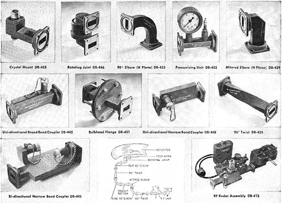
Waveguides’ flexibility shines in several critical domains of microwave communications. In military defense realms, they’re core to radar systems on land, sea, or air platforms by accurately focusing microwave energy for precise target identification and pursuit. Civil aviation also depends on these devices. Air traffic control radars leverage waveguides to monitor and orchestrate the movement of various aircraft types—from commercial liners to private jets—and even include military flights within controlled airspace. To enhance performance during high-power transmissions, engineers may pressurize waveguides with gas to ward off electrical discharge while installing specialized windows at their terminals that prevent moisture intrusion but allow uninterrupted signal flow—illustrating how adaptably waveguide technology meets today’s stringent demands in advanced microwave communication frameworks.
Optical Fiber Networks
Optical fiber networks represent one of the most revolutionary applications of waveguide technology, fundamentally transforming global communications. At the heart of these networks are optical waveguides – hair-thin strands of ultra-pure glass or plastic that guide light signals over vast distances with remarkably low loss. This capability has enabled the creation of high-speed, high-capacity communication networks that form the backbone of the internet and modern telecommunications infrastructure.
The principle behind optical fiber waveguides is elegantly simple yet profoundly effective. The waveguide structure within fiber optic cables ensures that light waves remain confined within the core, preventing them from escaping and maintaining signal integrity over long distances. This confinement is achieved through the principle of total internal reflection, where the core of the fiber has a higher refractive index than its surrounding cladding.
The development of silica-based waveguides, which can be fabricated on silicon wafers, has further expanded the possibilities of optical communications, enabling the integration of optical components with electronic circuits. This convergence of optical and electronic technologies in waveguide form is paving the way for even faster, more efficient communication systems, pushing the boundaries of what’s possible in data transmission and processing.
Medical and Industrial Uses
Waveguide technology’s implementation across medical and industrial sectors underscores its broad utility and groundbreaking influence beyond the realm of communications. Within the domain of medical oncology, waveguides are instrumental in operating clinical linear accelerators for radiation therapy. These advanced devices leverage waveguide technology to meticulously steer high-energy electromagnetic waves used in treating cancerous growths, focusing on diseased tissue with precision that helps preserve adjacent healthy cells. This usage highlights the critical contribution of waveguides to enhancing patient care and propelling advancements in healthcare treatments.
To oncological applications, an array of other areas within medicine and industry also employ waveguides.
- Waveguides serve a vital function inside MRI systems by channeling radio frequency pulses necessary for crafting intricate images depicting internal body structures.
- In security screening contexts such as cargo inspection via X-ray scanners, they improve safety protocols integral to transportation logistics.
- The role played by waveguides extends into industrial processes like plasma cutting or welding operations where their sharp focus on directing electromagnetic waves facilitates precise and effective production methods.
The myriad uses mentioned above reveal not only the versatility but also significant contributions that can be attributed directly to waveguide technologies affecting diverse fields, including health services delivery, manufacturing innovation, and antiterrorism strategies focused on bolstering public safety initiatives worldwide.
Mathematical Analysis of Waveguides
The study of waveguides is deeply rooted in the mathematical analysis which is pivotal for grasping their operational principles and enhancing their configuration. Central to this scrutiny are Maxwell’s equations, the pillars governing electromagnetic fields’ dynamics. When these fundamental laws are applied to a waveguide’s particular geometry and its boundary conditions, they empower us with predictive capabilities about how electromagnetic waves will behave within that medium. This calculation structure is essential for identifying crucial factors such as propagation modes, distributions of the field, among other vital traits inherent to waveguides.
Adapting specific coordinate systems pertinent to a given waveguide’s shape simplifies complex analytical tasks associated with them. Rectangular coordinates come into play when examining rectangular waveguidives due largely to compatibility with their shape. Conversely, circular coordinates prove advantageous when delving into circular ones – all resulting in smoother mathematic expressions which pave way toward insights on waveform behavior inside those environments.
Exploration through mathematics uncovers a profound connection between physical attributes of a guide and its electromagnetism phenomena. Through an abstract lens, one could envisage a waveguide as setting boundaries upon the classical equation describing waves. It dictates zero-valued functions along confines yet allows unfettered propagative motion across another dimension altogether (often lengthwise). Grasping this notion affords a better appreciation concerning how various aspects like dimensions or contours can affect mode patterns followed by signals coursing down paths carved out by design intended wavelength operations coupled alongside polarization features dictated therein.
Hence arises an intricate dance amongst numerous elements determining efficacy at different spectral frequencies—thereby solidifying mathematical inspection not just relevant but critically indispensable towards tailoring specfic end-uses befittingly matching varied application needs surrounding any form of comprehensive channel construction efforts aimed at moving information bound via spectrum parcels classified under ‘electromagnetic’.
Practical Considerations
In the implementation of waveguide systems, a number of considerations come to the forefront that significantly affect their efficiency and reliability. Impedance matching is among these critical factors. It’s essential for efficient transfer of energy and reducing reflections by aligning the impedance between the waveguide, source, and load correctly. Failure in achieving proper impedance matching can result in standing waves within the waveguides that could harm the signal source while also diminishing system performance.
The structural soundness of a waveguide system is another vital practical consideration. Waveguides need to be adequately sealed against moisture to prevent corrosion on their inner surfaces which would impair conductivity as time passes. Although flexible corrugated waveguides provide some level of bendability, they usually are not chosen due to compromised propagation characteristics. Rigidly structured variants are preferred because they deliver more reliable microwave energy transmission with minimal losses, especially when compared with coaxial cable alternatives.
These operational concerns highlight how crucial meticulous design, adept installation procedures and ongoing maintenance are for securing maximum effectiveness and durability from waveguide systems across various uses.
Impedance Matching
The concept of impedance matching is vitally important in the engineering and utilization of waveguides, as it greatly influences energy transfer efficiency and signal reflection reduction. When a waveguide’s impedance is appropriately aligned with that of its source and load, this alignment facilitates several outcomes.
- Enhancement of power transfer to its maximum potential
- Reduction in the amount of energy bounced back toward the origin point
- Preservation of signal integrity without degradation
- Avoidance of standing waves within the guide, which can otherwise create overheating issues or damage sophisticated gear.
For optimal functioning, achieving efficient operational conditions through impedance matching is indispensable for waveguides.
Reflecting on power transmission efficacy within these systems illuminates how crucial proper impedance pairing truly is. A well-matched setup has the capability to accomplish up to 50% effectiveness in directing power from source to destination. In contrast, discrepancies between impedances are likely culprits for creating voltage standing waves inside a conduit. Such peaks escalate voltages at particular junctures along a path. Not only do these spikes diminish overall performance, but they also present hazards for any equipment connected downline.
Given these factors—high stakes involving both function and safety—the precise calibration required by waveguide designs must be addressed thoroughly during their development phase using an array tailored tools like networks explicitly intended for matching or fine-tuning components designed specifically to align with specific frequency spectrums effectively.
Waveguide Plumbing
The concept of “waveguide plumbing” may initially seem unusual, yet it precisely captures the essence of installing and sustaining waveguide systems for uninterrupted signal transmission. Similar to how building plumbing demands close scrutiny to avert leaks and preserve fluid flow, waveguide plumbing requires exacting attention during the setup and upkeep of its components to avoid loss of signal and reflections. This is particularly vital in applications that operate at high frequencies, as small defects can substantially hinder performance.
For peak functionality, routine maintenance and inspections are crucial for these waveguides.
- Scanning for any signs of leakage
- Making sure there aren’t any sharp bends interfering with the propagation of signals
- Gauging Voltage Standing Wave Ratio (VSWR) as an indicator of system health
Extra vigilance against arcing must be given in powerful waveguide setups due to potential flaws like bumps or punctures within conducting surfaces—underscoring why thorough evaluation routines are critical.
It’s imperative to match the characteristic impedance within the guide itself with that which it loads. This synchronization optimizes power delivery while cutting down on losses stemming from standing waves. Thus effective ‘plumbing’ encompasses more than assembling physical parts—it includes preserving both electrical conduction continuity across all segments involved in signaling pathways.
Observing Guided Waves
Studying the behavior of confined electromagnetic waves inside waveguides is essential to improve their functionality and enhance their design. Tiny antenna-like structures serve as a means for introducing signals into the waveguides and drawing them out again. These elements may resemble short dipoles, stubs, or small wire loops affixed to the interior surface of the waveguide. Serving as conduits between external electronics and internal guided waves, these devices enable both signal injection and retrieval.
To scrutinize guided waves within these constructs, sampling probes or detection antennas are employed to measure electromagnetic fields at multiple locations along the path of propagation. Inserting slender receiving antennas like stubs or loops facilitates this pickup process within the confines of a guide. For comprehensive field analysis across its length—that includes detecting variations in intensity—these sensors can traverse through slots cut in the structure.
The application of such probing methods offers deep insights into how waves behave once contained by a waveguide’s boundaries. Particularly enlightening when exploring phenomena under different conditions. When injecting frequencies below that required by cutoff frequency thresholds associated with specific guides (the so-called “cutoff” frequency), it becomes clear how effectively they act as filters—the weakening signal discernible via sequentially positioned probe readings underscores this point sharply while traveling downwave from an insertion juncture closer upline confirms whether standing-wave patterns emerge due—as witnessed in scenarios where reflectivity defines terminal end dynamics vis-à-vis incident beams—and allows accurate determination regarding wavelengths characterizing those operative modalities prevalent therein—a boon for empirical confirmation relative towards theoretical forecasts integral toward attuning geometries adapted purposefully per definitive technological imperatives underpinning practical deployment strategies industrywide.
Advanced Topics
Delving deeper into the intricate world of waveguides introduces us to pioneering subjects that push traditional waveguide technology boundaries and explore novel methods for electromagnetic wave control. Nanoplasmonics and waveguide dispersion emerge as two particularly intriguing research areas at the forefront of this scientific endeavor, opening new avenues for light manipulation well below the optical wavelength level and shedding light on the intricate dynamics of waves in constrained environments.
As we investigate these sophisticated topics, we unlock their capacity to revolutionize multiple fields, encompassing telecommunications as well as nanoscale sensing and imaging applications.
Plasmonic Waveguides
Plasmonic waveguides are at the forefront of nanoscale electromagnetic wave guidance, redefining what we can achieve in terms of optical control and confinement. By utilizing surface plasmon polaritons — which combine the oscillations of both electromagnetic waves and free electrons on metal-dielectric interfaces — these waveguides compress light beyond the diffraction limit inherent to traditional optics. Such compression unlocks new pathways for ultra-miniaturized photonic circuits, advanced high-resolution imaging systems, and highly sensitive biosensors.
Yet developing plasmonic waveguides is accompanied by notable difficulties.
- The typically significant propagation losses linked to plasmonic modes may restrict how far signals can be carried.
- Ensuring effective entry of light into these minute configurations presents a challenge.
- Fabricating various active or passive photonics elements introduces complex engineering problems.
Nevertheless, due to their prospects for facilitating genuinely minuscule optical devices and networks, efforts continue to surge forward in perfecting plasmonic waveguide technology despite these challenges.
Advances in crafting methods coupled with breakthroughs in material science indicate that as progress marches on, plasmonic waveguides are set to become integral components within emerging nanophotonic tech—acting as crucial connectors between electronics and photonics on a diminutive scale.
Waveguide Dispersion
Dispersion within waveguides is an intricate occurrence, rooted in the characteristics of confined electromagnetic waves, which has a significant impact on optical communication system efficiency. It is characterized by variations in group delay per wavelength, causing the temporal widening of optical pulses during transit through a waveguide. In digital communications systems, this pulse broadening can create intersymbol interference that may constrain both the data transfer speed and reach.
In specific types of optical fibers and integrated photonics devices like photonic crystal fibers with limited mode volumes, pronounced effects from waveguide dispersion are evident. These include anomalous dispersion within the visible spectrum range—a phenomenon beneficial for certain uses such as generating supercontinuum light sources. Grasping and regulating waveguide dispersion is vital for developing advanced optical communication infrastructures and specialized light-processing components. To either dampen or harness these dispersive influences effectively requires employing tactics such as utilizing fibers designed to shift dispersion properties, implementing modules tailored for compensation purposes or precision designing of the physical structure guiding photons according to targeted application needs.
As demands escalate for augmented data throughput capacities along with increasingly sophisticated photonic circuitry designs, new horizons in optics technologies. Mastering manipulation over factors including control over manifold properties related to waveform spreading becomes progressively central to advancing our abilities surrounding managing operations at various wavelengths integral, especially those used across diverse spectrums operated via fiber optic transmissions systems among other potential areas leveraging optoelectronic advancements.
Waveguide manufacturing

The fabrication of waveguides is an intricate endeavor, involving the integration of exacting engineering practices with sophisticated material science to facilitate efficient guidance of electromagnetic waves. The selection process for materials in constructing waveguides is vital and largely hinges on the specific application and frequency spectrum it will serve. Frequently utilized materials comprise metals known for their outstanding conductivity such as copper, brass, and aluminum. These are ideal choices especially for guiding microwaves and millimeter-wavelength electromagnetic waves owing to their superior electrical characteristics coupled with ease of shaping.
A significant leap forward within the realm of waveguide production has been achieved through the introduction of cold-drawn tubing processes. This contemporary method delivers many benefits when contrasted with traditional manufacturing approaches.
- It yields greatly improved dimensional precision that ensures uniformity in electrical properties throughout a waveguide’s span.
- Cold-drawn construction bolsters mechanical robustness thus rendering them more adept at resisting distortion and coping with external stressors.
- This technique results in smoother inner surfaces which curtail signal loss while concurrently boosting efficiency.
Manufacturing nuances for creating waveguides differ based on both function and type desired. For metallic types like those used at microwave frequencies, common production techniques include extrusion methods, electroforming procedures along with precise cutting techniques—each offers distinct advantages regarding cost-efficiency measures or scale-up potential while keeping up performance tolerances required by applications’ specifications could be met. In producing dielectric versions relevant to integrated optics settings, utilize complex lithography exposure strategies combined with vapor deposition systems plus detailed etching actions as part of the fabricating sequence. Manufacturing strategy adoption becomes key as it bears direct influence upon numerous operational attributes inherent to a given guide—for instance its capacity related power handling considerations insertion dissipation figures plus range under conditions utilisation included.With each technological step taken new innovative means arise steadily transforming design possibilities extend operating limitations evermore capable delivery structures meant handle paths transmission energy form electromagnetism navigated therein.
Summary
In summarizing our journey through the domain of waveguides, it’s evident that these ingenious constructs are crucial in forging the infrastructure of contemporary technology. Covering everything from basic electromagnetic wave propagation to sophisticated matters such as plasmonic waveguides and dispersion control, we’ve recognized how integral they are across a spectrum of uses including communication systems, medical applications, industrial processes, and academic inquiry. The capacity for directing and managing electromagnetic energy effectively at various wavelengths is why waveguides have become so central to numerous technological areas like microwave transmission, radar frameworks, optical fiber channels, and state-of-the-art health equipment.
Continued innovation in the realm of waveguide technologies promises even greater advancement in manipulating electromagnetic waves. Looking ahead into what lies beyond today’s achievements suggests thrilling possibilities with new materials merging with progressive fabrication methods alongside original design concepts. All leading toward Enhancement within this field. Such developments hold great promise for accelerating data networks’ performance levels or pushing forward techniques used in medical diagnostics and treatments or even pioneering entirely fresh scientific insights – maintaining the standing position of wavegrades as an imperative component driving progress across multiple aspects related to connectivity improvements healthcare advancements plus broadened comprehension pertaining to our interaction with electromagnetism.